G lass interposer require s more fluence comp ared to organic interposer. The electrical properties of the glass substrate are as follows.
Polymers In Electronic Packaging Build Up Films For Flip Chip Semiconductor Substrates Part Two Polymer Innovation Blog
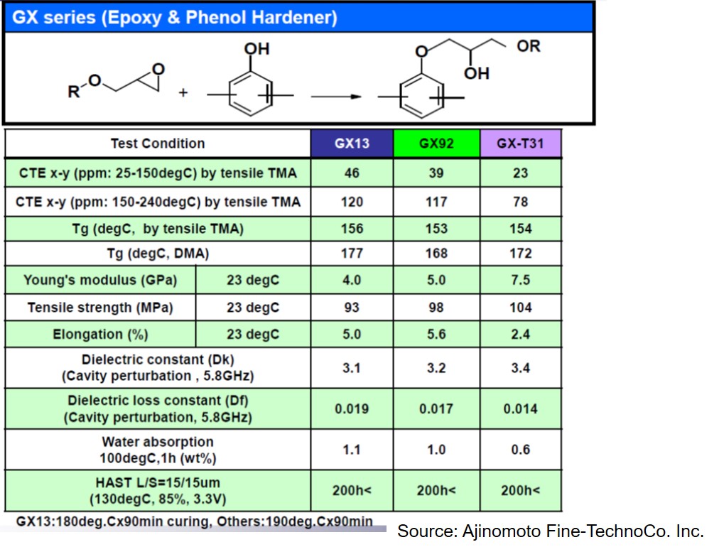
Melting viscosity of GX13 GX92 GXT31 The same facility and laminate condition is applicable for all variety.
Build material gx92 gl102. 0005 at 10 GHz. Number of Measurement Pad. Unfortunately this roughness also contributes to additional conductor loss.
SummaryA properly designed and optimized SAP metallization process is capable of delivering excellent results not only on current generation materials but also on next-generation build-up dielectric materials such as Ajinomoto ABF-GX92 and GZ22The use of a single SAP process with capability for both current and future generation materials allows IC substrate manufacturers to. Cu OSP option solder coat Electroless NiAu. Advent of Ajinomoto Build-up Film ABF an interlayer insulating material for semiconductor packaging 1950s RD on MSG synthesis MSG.
What is interesting to note is the trend to thinner BT-epoxy cores and eventually to a coreless package. For g lass interposer the experimental outlook is shown in Table 4. Melting viscosity Poise degC GX13 1900 135 GX92 3700 131 GXT31 3600 129 Ajinomoto Build-up film.
Each pulse removes a certain amount of material Etch-rate material removedpulse With a known etch-rate the number of pulses to reach a desired depth can be predicted and controlled Selective Material Removal. GX92 GX-T31 GZ41 GL ¼ º ª 04412 30 2 W H t H t Z r s H S Formula of strip line impedance W45-50um 2H80um t13-23um Z S50Ω Low Df material shows lower transmission loss. 100degC 30s vac 30s rubber press 7kgfcm2 Air 2nd.
Assume Typical Polyimide Etch-rate 030 m pulse. 10a surface mount glass passivated bridge rectifier reverse voltage dongguan you feng wei electronics co ltd abf2. PKG Thickness mm 055 047.
It is not commonly known that the Ajinomoto Group provides a benchmark component of computers. Figure 2 shows the evolution of build-up materials. Center Area 18x20 Matrix Corner Area 19x20 four Matrix.
Electro-deposited ED copper is widely used in the PCB industry. The manufacturing process sees a large rotating drum made of polished stainless steel or titanium which is partially. The new materials are also targeting the needs of coreless build-up substrates.
Core Hitachi E679FGR E700GR E705G E705GLH Panasonic R1515SL R1515A R1515W MGC HL832NSF. GX92R 40um Test board TH substrate 03mmtTH f250umpitch 500um Procedure 1. The organic materials are processed directly by the irradiation using the mask by 248 nm excimer laser.
Organic interposer material processing test condition. The material stackup consists of ultra-thin 100-μm EN-A1 glass substrate from Asahi Glass Co AGC laminated with 15-μm Ajinomoto ABF GL102 on both sides. Abf1 datasheet surface mount glass passivated bridge rectifiers - hy electronic corp.
Similarly the electrical properties of ABF GL102 are. 100degC 60s SUS press 55kgfcm2 2. Die Thickness um 40.
150-240degC by tensile TMA 120 117 78 Tg degC by tensile TMA 156 153 154 Tg degC DMA 177 168 172 Youngs modulus GPa 23 degC 40 50 75. In this method it is possible to process fine patterns and various patterns. 25-150degC by tensile TMA 46 39 23 CTE x-y ppm.
Ww22 2019 Proprietary and Confidential of AJICO 11. 2011 GX92 ABF Ajinomoto Build-up Film build-up layers. Surface Spec of Electrode.
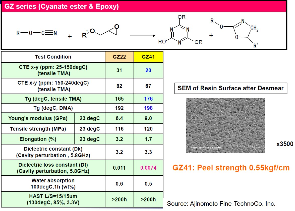
The types of ABF were GX92 GX-T31 and GY50 and their thickness was 10 μm. Next build-up material in demand 5302013 10. Test Condition GX13 GX92 GX-T31 CTE x-y ppm.
Curing w PET and wo PET 100degC60min180degC30min. In fact Ajinomoto Build-up Film ABF can be found at the heart of most of the worlds personal computers where it provides electrical insulation of complex circuit substrates for high-performance central processing units CPUs. Metal pads 1µm thick are a Stop Layer 65º 81º Example.
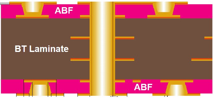
The schematic in the top right image depicts a very high density ball grid array BGA semiconductor substrate most likely used for high density flip chip applications FC-BGA. We processed using Ajinomoto build-up films ABF as organic material. TH Plugging by GX92R Ajinomoto Build-up film Variety.
Origin of Electronic Materials Business Interlayer insulating material for semiconductor packaging has its origins in technology used to develop epoxy resin curing agent Epoxy resin curing agent 1999. Dielectric constant Dk 54 and loss tangent Df. Interposer material Ajinomoto Build up Film ABF GX92 and GY50.
Ajinomoto are now working on next generation materials with high Tg low Dk and low CTE to meet the low loss and performance requirements of future semiconductor substrates. 30 25.

Polymers In Electronic Packaging Build Up Films For Flip Chip Semiconductor Substrates Part Two Polymer Innovation Blog
Http Www Ectcregistration Net Files 69 Ectc2019 20presentation 20material Ajinomoto Pdf
Https Ieeexplore Ieee Org Iel7 9006769 9026560 09026708 Pdf
Polymers In Electronic Packaging Build Up Films For Flip Chip Semiconductor Substrates Part Two Polymer Innovation Blog


Polymers In Electronic Packaging Build Up Films For Flip Chip Semiconductor Substrates Part Two Polymer Innovation Blog
Http Www Ectcregistration Net Files 69 Ectc2019 20presentation 20material Ajinomoto Pdf
Http Www Ectcregistration Net Files 69 Ectc2019 20presentation 20material Ajinomoto Pdf
Https Www Semitracks Com Newsletters October 2015 October Newsletter Pdf

Development Of Fcbga Substrate With Low Dk Df Material Based On Automotive Reliability Conditions Semantic Scholar


Http Www Ectcregistration Net Files 69 Ectc2019 20presentation 20material Ajinomoto Pdf


Development Of Fcbga Substrate With Low Dk Df Material Based On Automotive Reliability Conditions Semantic Scholar
Https Www Semitracks Com Newsletters October 2015 October Newsletter Pdf
Comments
Post a Comment